
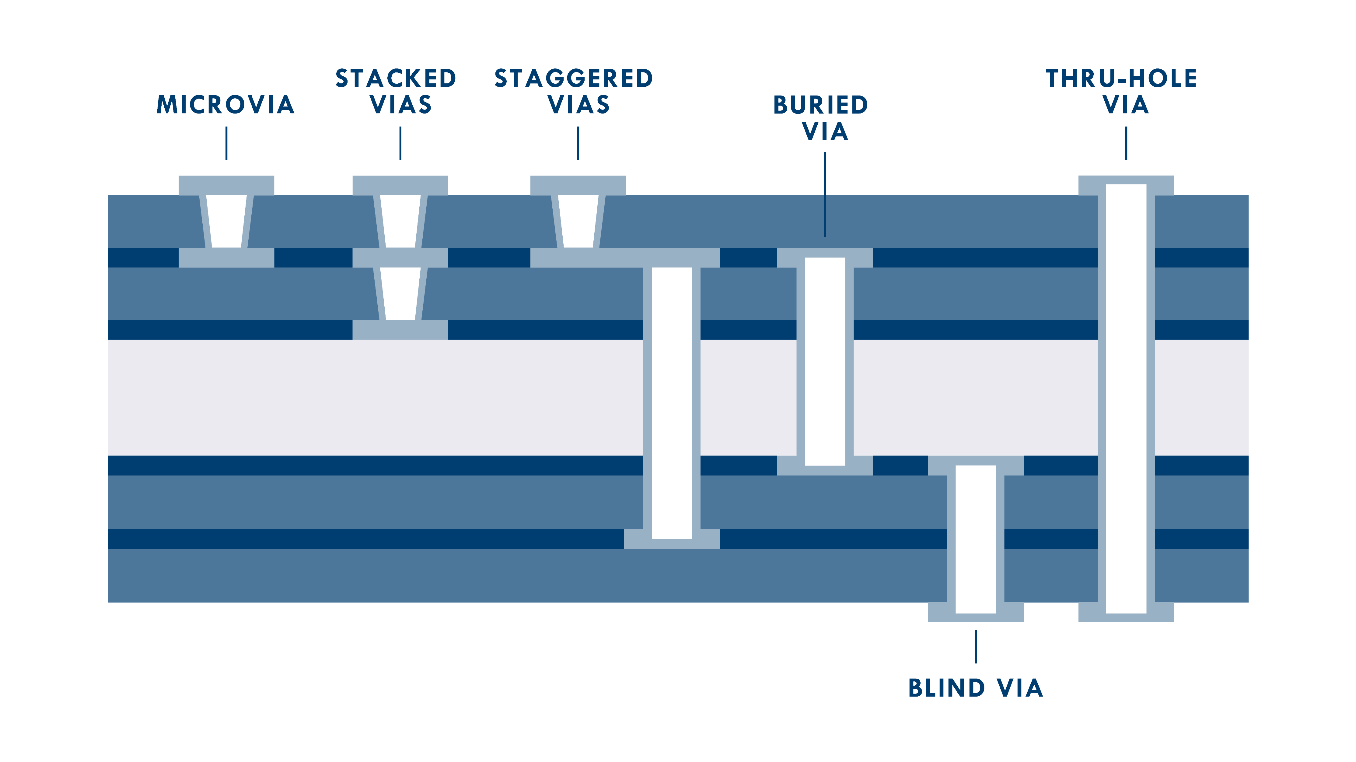
An essential design element in printed circuit boards, vias enable electrical connections between different layers of a circuit. Each type of via has its advantages and is chosen based on the specific requirements of the circuit board design, including factors such as space constraints, signal integrity, thermal management, and manufacturing cost.
1. Through-Hole Vias (PTH – Plated Through-Hole):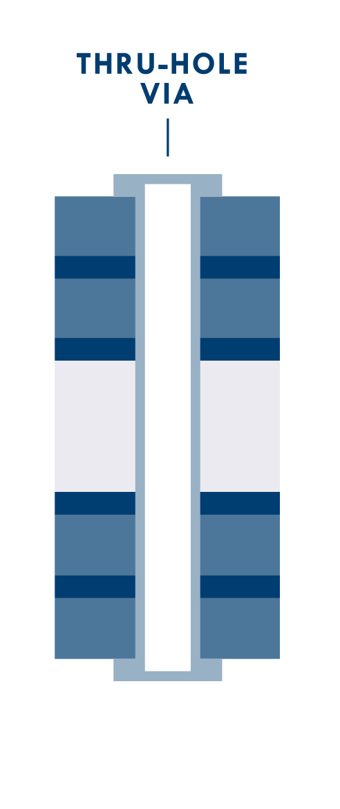
- Most common type of via
- Extend completely through the circuit, connecting traces on different outer layers.
- Sturdy and reliable, suitable for most applications.
- Used for power and ground connections, as well as for mounting components that require mechanical supp
- Larger Board Size: PTH components and vias necessitate drilling holes, which increases the board size and limits available space for routing.
- Better Heat Dissipation: The larger size of PTH vias as compared to microvias, allows for better heat transfer away from components. This can be important for high-power applications.
2. Blind Vias: 

- Connect an outer layer of the circuit to one or more inner layers
- Do not extend through the entire circuit board.
- Used when traces need to be connected to inner layers but don’t require connection to the opposite side of the circuit.
- Save space
- Used in high-density circuit board designs where space is limited.
- Limited Re-workability
3. Buried Vias:
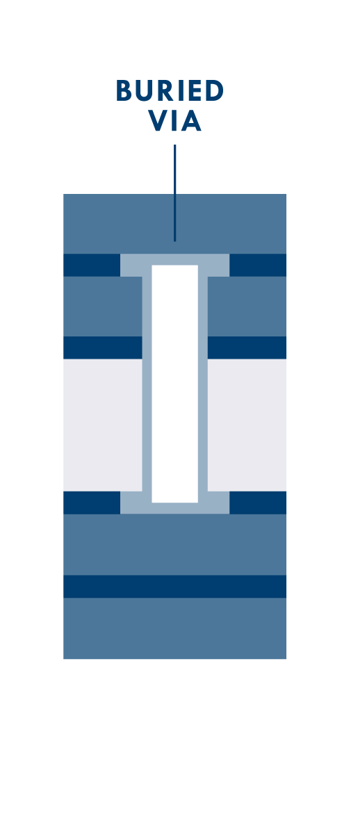
- Fully contained within the layers of the circuit and do not extend to the outer layers.
- Connect one or more inner layers of the circuit but are not visible from the surface.
- Used to increase circuit board density and reduce signal interference by providing additional routing layers without increasing board thickness.
4. Microvias:
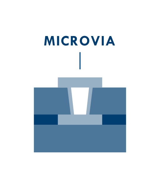
- Typically less than 0.15mm or 6 mil in diameter.
- Used in high-density interconnect (HDI) circuit boards to create finer pitch traces and increase routing density.
- Enable smaller, lighter, and more compact electronic devices by allowing for more efficient use of circuit board space.
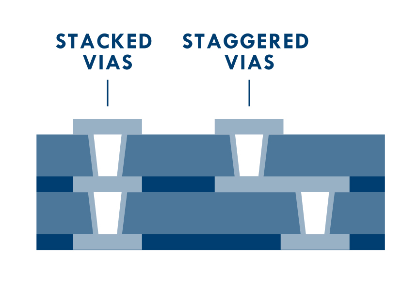
- Microvias can be Stacked or Staggered for higher density designs.
- Reliability Concerns: More prone to defects during fabrication, such as plating issues, which can lead to reliability problems down the line.
- More Expensive: Microvias generally cost more to manufacture than traditional through-hole vias. This is because the fabrication process is more complex.
- Potential for Lower Power Handling: Smaller cross-sectional area for current to flow, limiting the amount of power they can handle compared to larger vias. However, this isn’t always the case. With careful design and proper via selection based on the application’s current requirements, microvias can handle significant power.
5. Unfilled Vias:
- It’s cost-effective and sufficient for many applications.
- Simpler Manufacturing: This can lead to faster turnaround times and potentially higher yields (fewer defects).
- Potentially Lower Electrical Resistance
- Limited Thermal Performance: Unfilled vias don’t contribute significantly to heat dissipation.
 and sufficient for many applications.
6. Filled Vias:
- Filled with conductive or non-conductive material after they are drilled.
- Conductive filled vias enhance reliability and thermal conductivity.
- Non-conductive filled vias improve planarity and surface finish.
- Higher coefficient of thermal expansion mismatch: (CTE) is a measure of how a material expands with heat. The CTE of the filling material might not perfectly match the surrounding laminate, causing stress on the via and the surrounding layers during temperature fluctuations, potentially leading to reliability issues.
- Commonly used in high-reliability applications such as aerospace and automotive electronics.
 conductive or non-conductive material after they are drilled.
 Contact us if you have questions about which type of via is best for your upcoming projects.
Work with your fabricator or manufacturing partner to understand what types of vias are appropriate for your next project.